The Grid Used In A Pcb Layout Tool Should Be
In metric (mm) in imperial (mils) both a and b interchangeably; Pcb designing fundamentals mcq questions and answers quiz.
enjoy discount GK64X DIY Mechanical Keyboard kit hot
Earlier, designers used to draw the circuit diagram on paper.

The grid used in a pcb layout tool should be. The software aims to better help with board design. In the layout you may use different values, for example 0,635mm and alternatively 0,05mm. Schematic (left) and board editors both open.
The grids in pcb design systems can be a very effective tool for organizing the creation of your design so that it looks the way you intended it to. Opening the project should cause two more eagle windows to spawn: The grid used in a pcb layout tool should be a.
Either a or b 10. A good grid value for the schematic is 0,635 mm which is 1/40 inch which is 25 mil. Select tools > verify design.
Usually, you’ll find two types of grids in a pcb editor. The biggest factor when it comes to impedance is a. The grid used in a pcb layout tool should be a.
The pcb layout elucidates how which and where components have to be connected. The solder paste files are generally produced. Both a and b interchangeably d.
A schematic diagram is a logical and visual representation of an electrical circuit. Schematic drawing sheet and border editor. The use of 3d component models in the pcb layout can assist with.
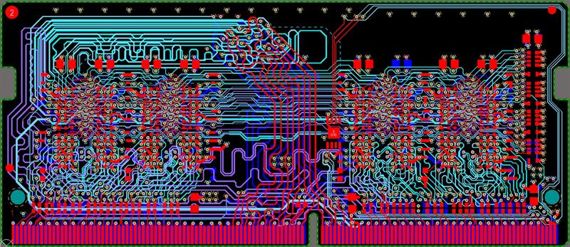
Pcb designing tools to design these kind of pcb we need some software.these kind of software’s are know as computer aided software tools. So you’ve got an idea for a circuit and would like to turn it into a printed circuit board (pcb)—but you don’t do it often enough to justify buying an expensive circuit layout program, and faced with learning how to use a pcb design tool is just too daunting. A printed circuit board (pcb) layout, is a soft design of traces, holes, and vias that have to be developed on the physical board for circuit development.
From the 1960’s through the 80’s the primary pcb desi gn grid system used imperial units. Components are based on this grid. Either a or b reason:
These are the yin and the yang of eagle. A 0.05 grid, and 0.005 alternate grid is a good size for this kind of board. The board and schematic editors.
The integrity of the signal from the output buffer of the sending component c. The first type is the viewing grid, which overlays on the layout to give you a sense of space and measurement as you work on the design. There are two parts to this:
Pcb artist is just one of many pcb layout software tools available to use, but an understanding of one layout tool can easily transfer to any pcb design tool. Tool to calculate track widths, and many other things. One small step for eagle, one giant leap for your pcb layout.
Some of the popular tools available are: They should be used together to create the finished product that is a functional pcb design. Though schematic tools do have to use a grid for pin connectivity, in theory, the grid used in a schematic is.
Units on the grid matter, as if the grid dictates that two wires are 10mm away from each other, then when you get that board manufactured, those two wires will be 10mm away from each other. Page size, borders) of your schematics. It is the very first step of electronic product design.
Sticking to a particular grid is highly recommended, as bouncing between grids will introduce tolerance and rounding errors. 3.4 verify your design you should now run a design check to ensure there are no routing errors with your design. The grid should be visible in the board editor.
Either a or b 17. The second type of grid generally referred to as the snap grid, is an important tool to create a meticulous layout. Smart grid technologies result in a more efficient and reliable system.
The pcb, by its nature, represents a physical device. Pcb artist is a free software tool and can be downloaded for free at www.4pcb.com. Using the proper grid size and units is essential:
All pcb design features and grid layouts were in 0.001” (1 mil) increments and everythi ng was symmetrical and evenly balanced. One small step for eagle, one. Your object that might have been originally off center of your grid should have snapped to a center origin point, and you’re done!
The solder mask has an impact on the trace impedance. Whether you need to align or distribute a group of components, vias, or pads, the new. Cursor snaps on grid [f6] should also remain activated in the schematic!
Eagle forces your parts, traces, and other objects to snap to the grid defined in the size box. Your object that might have been originally off center of your grid should have snapped to a center origin point, and you’re done! Then in 1988 the world standards organizations banded together to agree that the metric unit system was superior for solving pcb design development.
Clock speed of the board crystal b. In fact, the smart grid market, which was valued at over $30 billion in 2017, is expected to grow at an 11 percent compound annual growth rate (cagr) to reach $70 billion by 2024. The only restriction is that pcb artist will not output a gerber
The grid used in a pcb layout tool should be. Using the grid is very valuable in lining up components to look neat and orderly as well as drawing in nets that are not congested and confusing. You’ll first want to pull in a design block or part library to your design, and then select it with the group tool.
Eagle(easily accessiblegraphical layer editor) ki cad orcad diptrace altium designer dxdesigner ares factors a pcb designer should keep in mind : Pcb design tutorial part 1. Take the schematic for instance.
Tool to build a footprint or a component from a b&w bitmap image to create logos. A software design tool should need and have, there. It is because most of the target 3001!
Select tools > autoroute > start to begin the autoroute process. The software comes with everything; After a few seconds, the design should be fully routed as shown below.
The results of the test will appear in the. There are two different units used by kicad (and most other pcb ecads): Both a and b interchangeably d.
I actually use both, in the same design sometimes, if i have a mixture of metric and imperial parts. Used to edit the page layout and format (ie. An average pcb has several components, multiple connections, and holes.
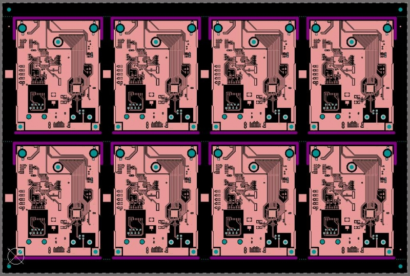
PCB Panelization Using The Embedded Board Array Altium
Electronics design tools and PCB design software
Altium Designer 18 to tackle even the most complex PCB designs
An Overview On Printed Circuit Boards Avanti Circuits

Top 12 Best Free PCB Design Software (2022)

What is the use of microcontrollers in design? Jotrin

SQL Workbench/J User's Manual SQLWorkbench
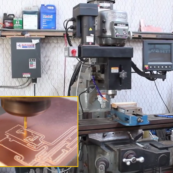
A Guide to Milling PCBs at Home Al día Noticias Roldanillo

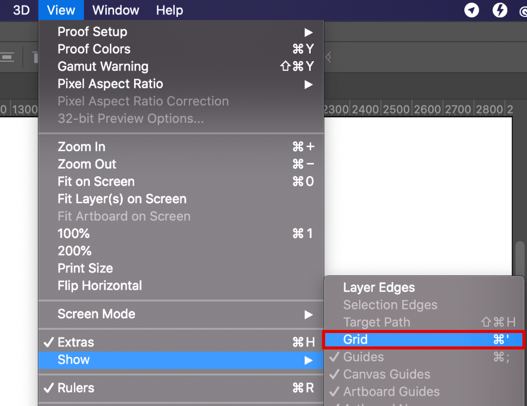
How to Use Grids and Guides
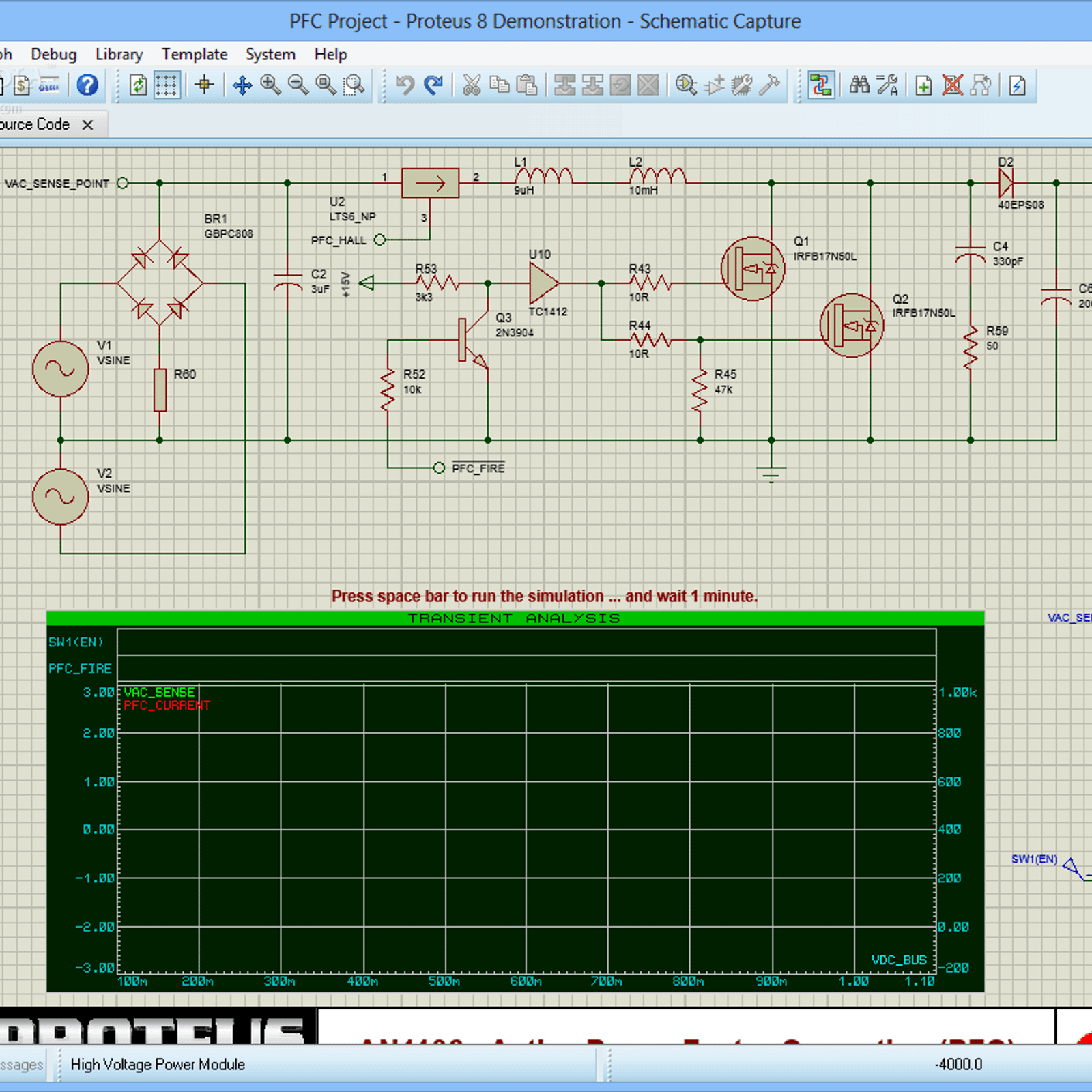
Proteus For Mac Free Download
enjoy discount GK64X DIY Mechanical Keyboard kit hot

Transducer Measuring Distance Module Ultrasonic Sensor

Inverter Diagram fixing a refrigerator compressor that

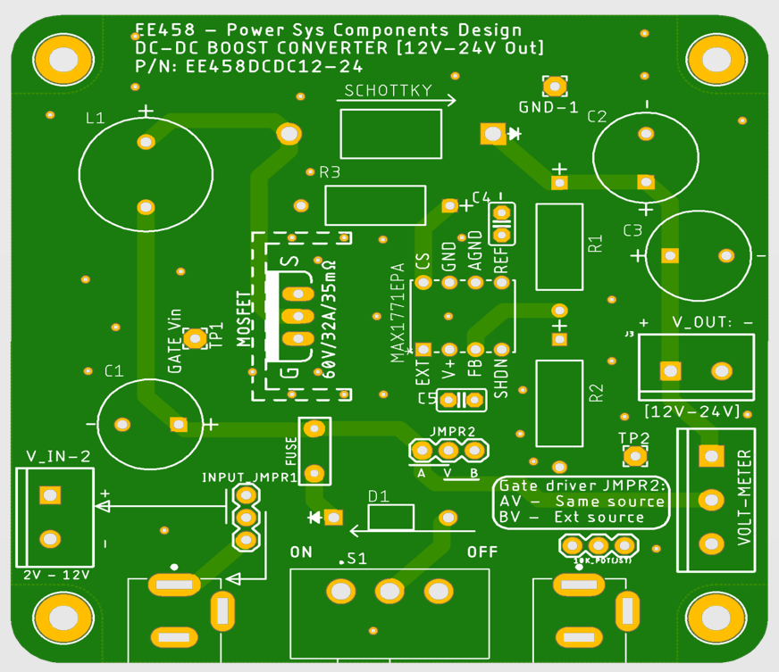
Boost converter
Electrical Engineer at Wavetronix

Printed Circuit Board Design, Diagram and Assembly Steps

A Guide To Milling PCBs At Home Hackaday
Grid Portals A User s Gateway to the
PCB Layout Basics Component Placement EAGLE Blog
